Restoring a Commodore CBM 3016
enWe recently got our hands on a Commodore CBM 3016, built between 1978 and 1980. Unfortunately, as we attempted to power it up, we were greeted with a screen full of random characters:
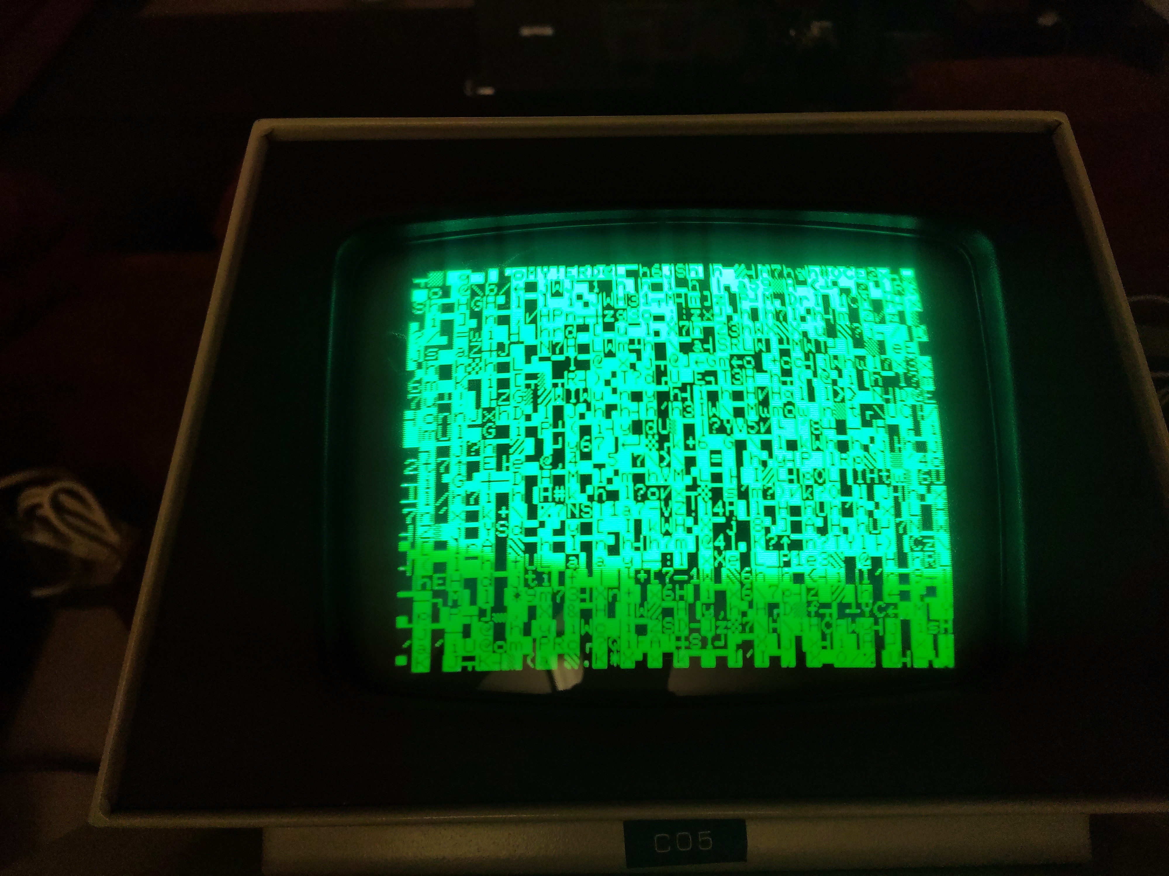
A short web search told us that a common cause for this issue are bad ROM modules.
Understanding the CBM Memory Layout and ROM
The MOS 6502 CPU used in the PET / CBM series has a 8 bit data bus and a 16 bit address bus. Schematics found online reveal that the uppermost 4 of those 16 bits are used to determine which device to talk to: The entire lower half of the address space ($0000:$7fff are mapped to DRAM, though on our model 3016 with 16KiB RAM, only the area $0000:$3fff can actually be used. Next follows the video buffer at $8000:$8fff, and after that follow different 4KiB ROM chips at $9000:9fff through $f000:$ffff. Again, only part of this is used; the address space $9000:$bfff maps to empty sockets which can be populated with software ROMs by the user.
The actual operating system of the CBM is stored on 4 different ROMs:
$c000:$cfff: BASIC editor/interpreter/runtime, part 1$d000:$dfff: BASIC editor/interpreter/runtime, part 2$e000:$e7ff: IO processing routines. This is actually a 2KiB ROM, the upper half is mapped to actual hardware IO (e.g. the keyboard).$f000:$ffff: The KERNAL ("kernel" with a typo that kept on living).
There also is an additional ROM, which stores the character set that can be displayed on the screen, but this ROM is not attached to the MOS 6502 address bus. Instead it is used directly by the screen rendering part of the PCB.
We removed these ROMs and dumped each of them using the MiniPRO TL866A programmer:
minipro -yp 27C32A@DIP24 -r basic1.bin
minipro -yp 27C32A@DIP24 -r basic2.bin
minipro -yp 27C32A@DIP24 -r kernal.bin
minipro -yp M2716@DIP24 -r io.bin
minipro -yp M2716@DIP24 -r chars.bin
Multiple versions of the KERNAL+BASIC system have been spotted in the wild, and we did not know which version was used by our CBM, so we didn't yet know what these dumps were actually supposed to look like. Fortunately, we managed to find dumps of most of these versions online, and only one of those matched our dumps: The BASIC 2.0 version.
At least most of our dumps matched. The IO ROM and the first BASIC ROM did not even closely resemble the dumps we had found online. Additionally, when we attempted to dump the ROMs for a second time, these two ROMs yielded totally different data. After repeating this for a few times, we concluded that these two ROMs were broken completely.
Creating New ROMs
We managed to find some pinout-compatible EPROMs we wanted to use as a replacement. However, after erasing them with our UV eraser, it turned out that our programmer was not capable of producing the 25V required for programming these chips. We fiddled around with an external PSU, and did achieve some success (as in: we managed to write some random bits), but we never managed to complete a full write sequence.
We started looking for alternatives and found multiple rails of AT27C040 PLCC-packaged one-time-programmable ROMs. These PROMs feature a whole 512 KiB of storage. Our plan was to use the lowermost 2 resp. 4 KiB and after programming short the excess address pins to GND. I designed a small adapter PCB from PLCC32 to DIP24, suitable for replacing both a 2K and a 4K ROM.
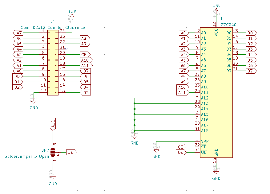
The solder bridge in this schematic is used to choose between the 2K and 4K version; with 4K the OE (Output Enable) pin of the ROM is always pulled low, for the 2K version it is connected to A11 (the 12th address bit): when this bit is HIGH, the output is disabled and the pins are kept floating as to not disturb the communcation between the CPU and the IO hardware mapped to the upper half of the $e000:$efff address space.
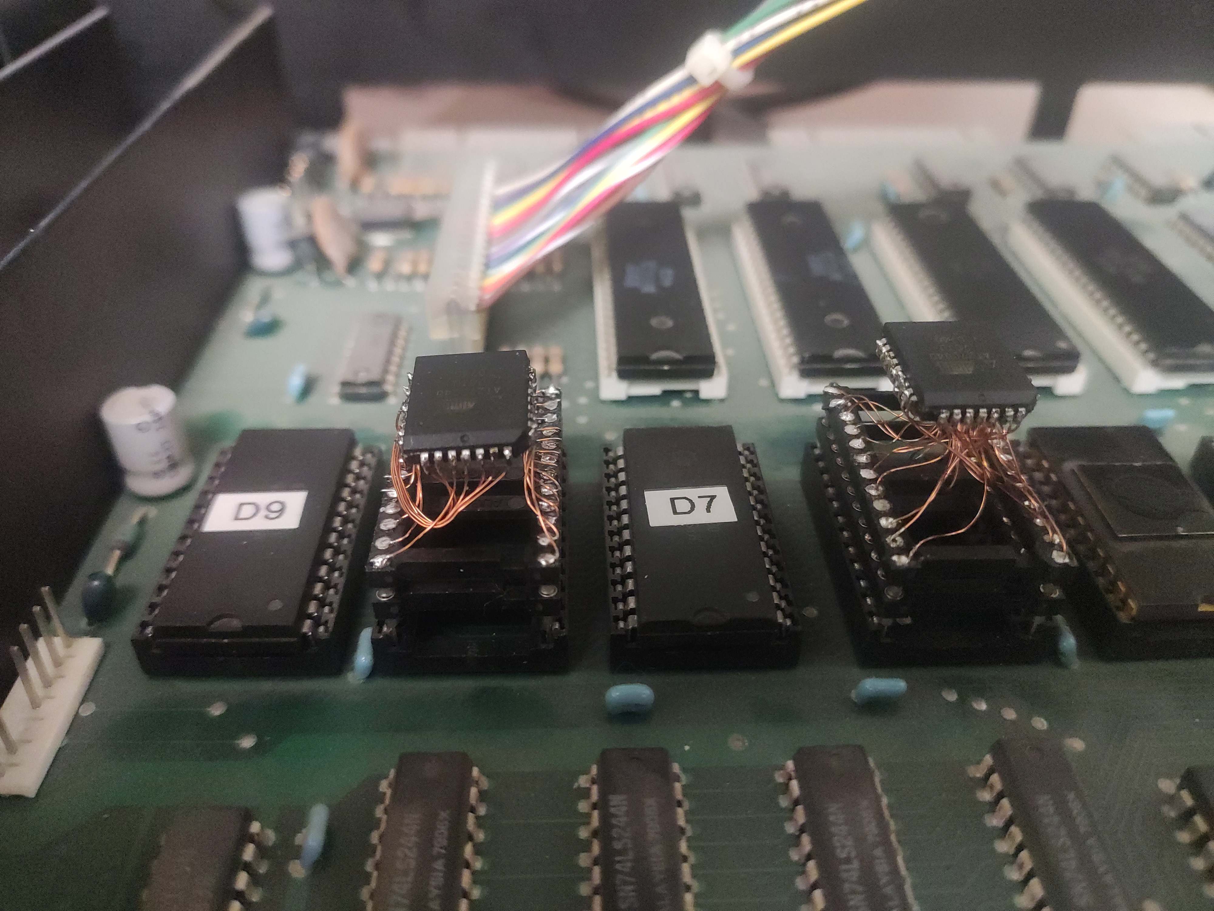
Though, in the end we used the ugly but easy solution of soldering some short wires between the ROM and a DIP socket, rather than manufacturing a full-blown PCB. And indeed, once we had put our replacement ROMs into their sockets, we did at least achieve some progress: The screen was still showing random characters on startup, but after a few seconds the entire screen was cleared, and then nothing happened anymore. So it appeared the CPU was doing something, but apparently not the right thing.
Hunting Down CPU Misbehavior
In order to figure out what the CPU was doing, I attached a logic analyzer to the address bus pins and recorded every address on the bus between startup and the screen blanking. One thing that became apparent immediately was that all communication on the address bus stopped after the screen was blanked. As the MOS 6502 CPU has to at least fetch an instruction every 1-6 cycles, it appeared as if the CPU had halted, which under normal conditions is only possible when it's executing a HCF-style illegal opcode.
So I took a closer look at the instructions the CPU was loading right before freezing. I used the dxa65 disassembler to turn the ROM dumps into 6502 assembly mnemonics in order to understand which instructions were located at which addresses. And indeed, the last instruction executed before freezing, read from address $f4e0, was $d2, an illegal opcode that halts the CPU. The disassembly revealed that this was actually not supposed to be an instruction, but a zeropage address passed as an argument to a previous instruction. Going a few cycles backwards, I found something that seemed promising: A rts (return from subroutine) instruction was loaded, followed by two accesses in the stack page at $01fe:$01ff (popping the return address from the stack), and then the next instruction was loaded from $f4d8. The odd part here is that a rts should only ever jump back to an address preceded by a corresponding jsr (jump to subroutine) instruction, which was absent here.
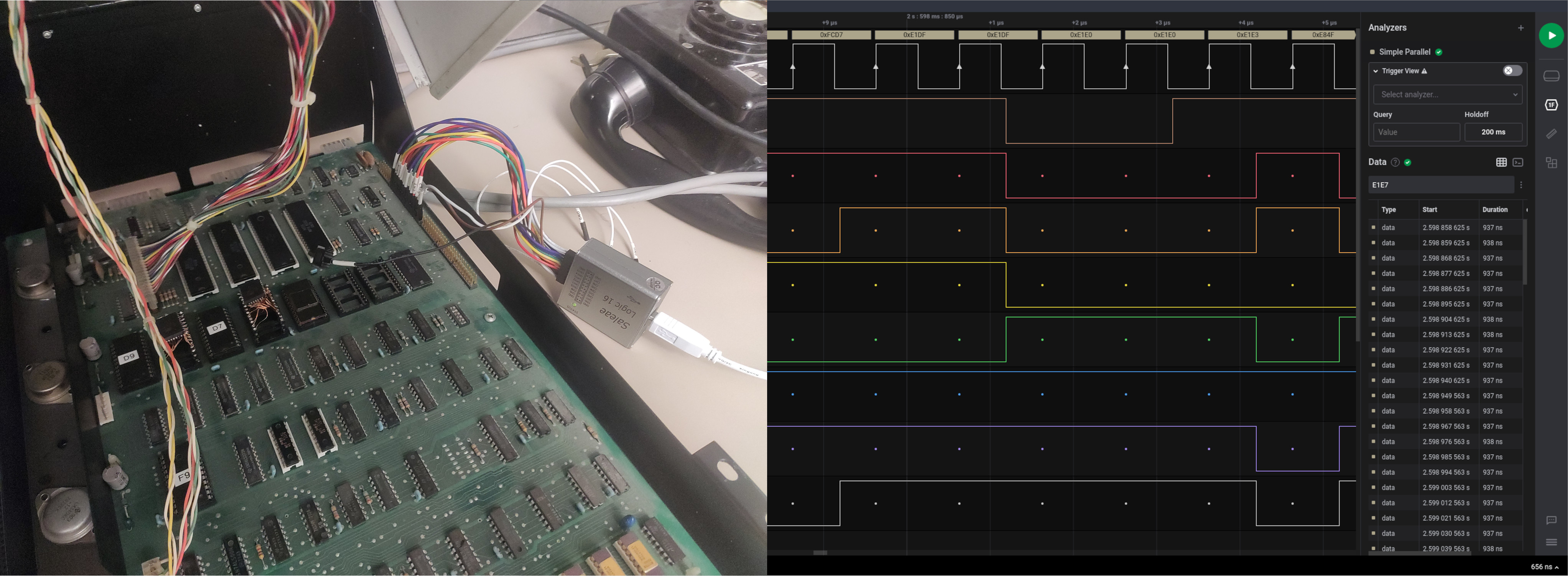
So clearly the CPU was returning to a wrong address. At this point I started to suspect faulty RAM. To find out more I searched even further back until I found the jsr instruction — at address $fcd5. So, according to the specification of the jsr instruction, the real return address pushed to the stack had to be $fcd7 (address of the jsr + 2). When we compare this to the address actually popped from the stack, $f6d7 (actual return address - 1), we can see that these addresses differ in exactly one bit, which confirmed my suspicion of faulty RAM:
$fcd7 = 1111 1100 1101 0111
$f4d7 = 1111 0100 1101 0111
             ^
Finding the Faulty RAM
In order to figure out which part of the RAM was broken, we first need to understand the DRAM chips' physical layout on the PCB.
The CBM 3016 series' DRAM consists of 16 MOSTEK MK4108 modules, each in a DIP16 package, organized in 2 groups of 8. Reading the datasheet of the MK4108/4116 (p.140ff), reveals that each one stores 8K single bits. Probing around on the PCB with a multimeter revealed the following memory layout:
               D0    D1    D2    D3    D4    D5    D6    D7
               __    __    __    __    __    __    __    __
              |  |  |  |  |  |  |  |  |  |  |  |  |  |  |  |
              |  |  |  |  |  |  |\/|  |  |  |  |  |  |  |  |
$0000:$1fff   |  |  |  |  |  |  |/\|  |  |  |  |  |  |  |  |
              |__|  |__|  |__|  |__|  |__|  |__|  |__|  |__|

               __    __    __    __    __    __    __    __
              |  |  |  |  |  |  |  |  |  |  |  |  |  |  |  |
              |  |  |  |  |  |  |  |  |  |  |  |  |  |  |  |
$2000:$3fff   |  |  |  |  |  |  |  |  |  |  |  |  |  |  |  |
              |__|  |__|  |__|  |__|  |__|  |__|  |__|  |__|


                            VVVV  FRONT VVVV
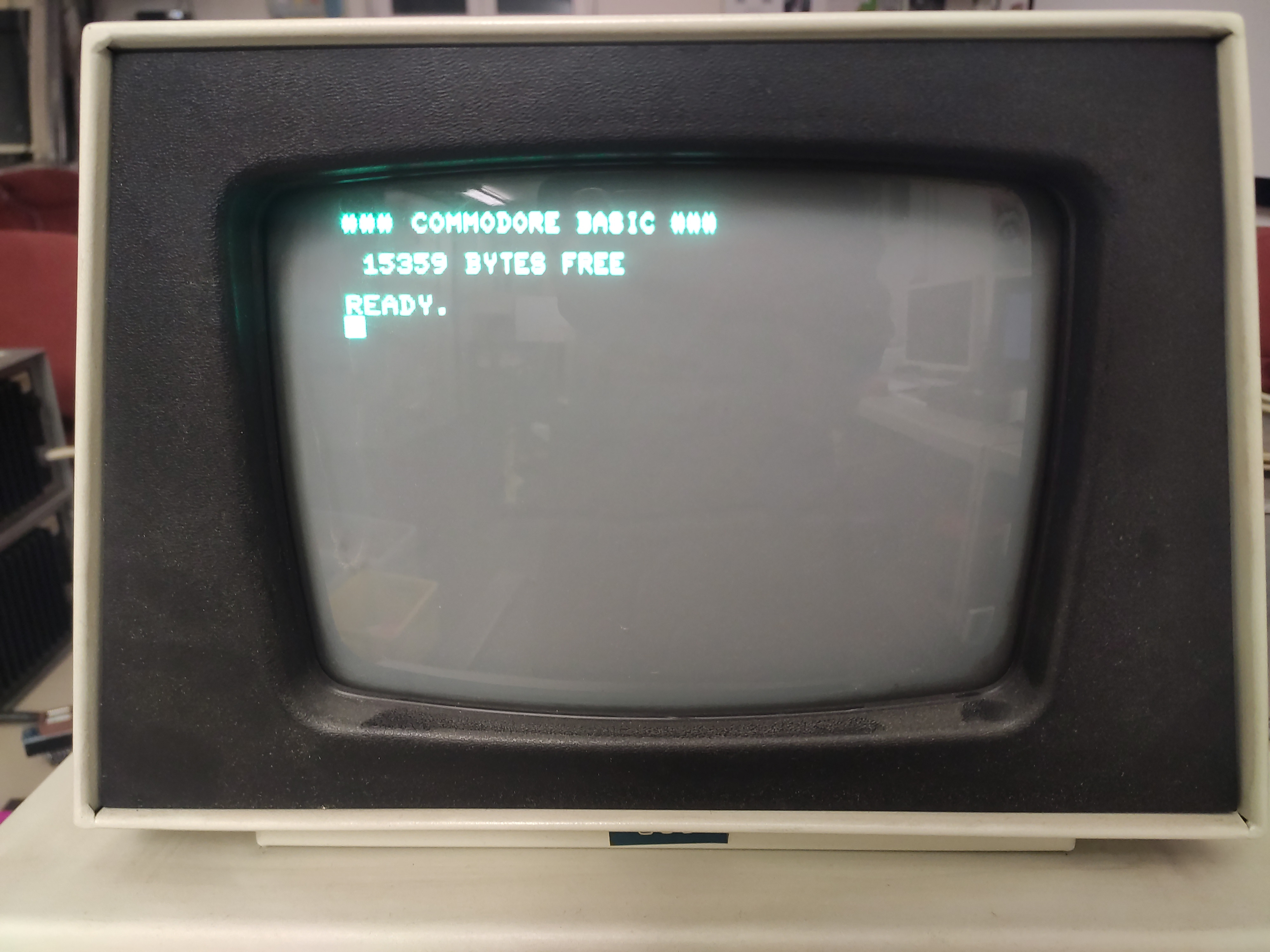
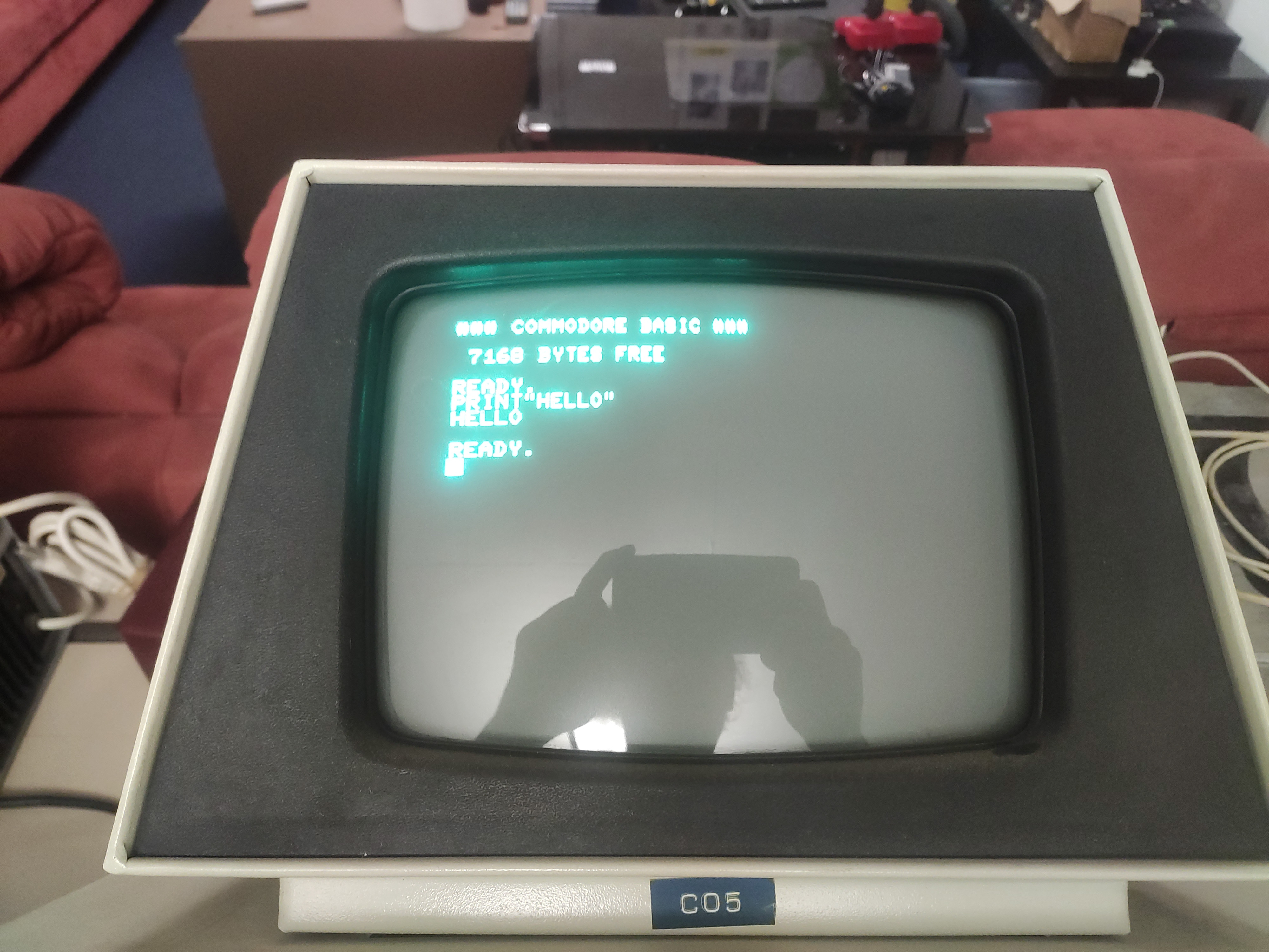
Since the flipped bit was in the 4th position (counting from the LSB of the upper byte), and the stack (where the wrong return address was read from) is at $0100:$01ff, the faulty module should be the D3 module in the upper row, marked with an X. To validate this, we swapped the module with the D3 module in the front row - luckily these DIP modules are socketed. Lo and behold, the computer started and we were presented with the BASIC interpreter. Note that instead of the usual ~15K memory, only 7K are reported as free and usable:
Now that the system had at least some working memory, I decided to write a small memtest program. I ended up writing this directly in 6502 assembly, written to a ROM plugged into the $f000:$ffff socket normally occupied by the KERNAL ROM, due to multiple reasons:
- The KERNAL actively uses the memory region
$0000:$2000, so loading the memtest program from another location after the KERNAL has been loaded would corrupt this memory region. - An entire memory page is occupied by the stack, but this page should be tested as well. Writing in assembly allowed me to avoid implicitly using the stack, or any other implicit memory allocations.
The memtest program only uses 7 bytes of zeropage memory to keep its state, the entire remainder of the memory is tested. For more efficient testing (and to not waste tons of single-write PROMs) I also ended up wrapping a MOS 6502 emulator with the CBM 3016's memory map and simulated memory failures. The memtest program can be found on Gitlab.
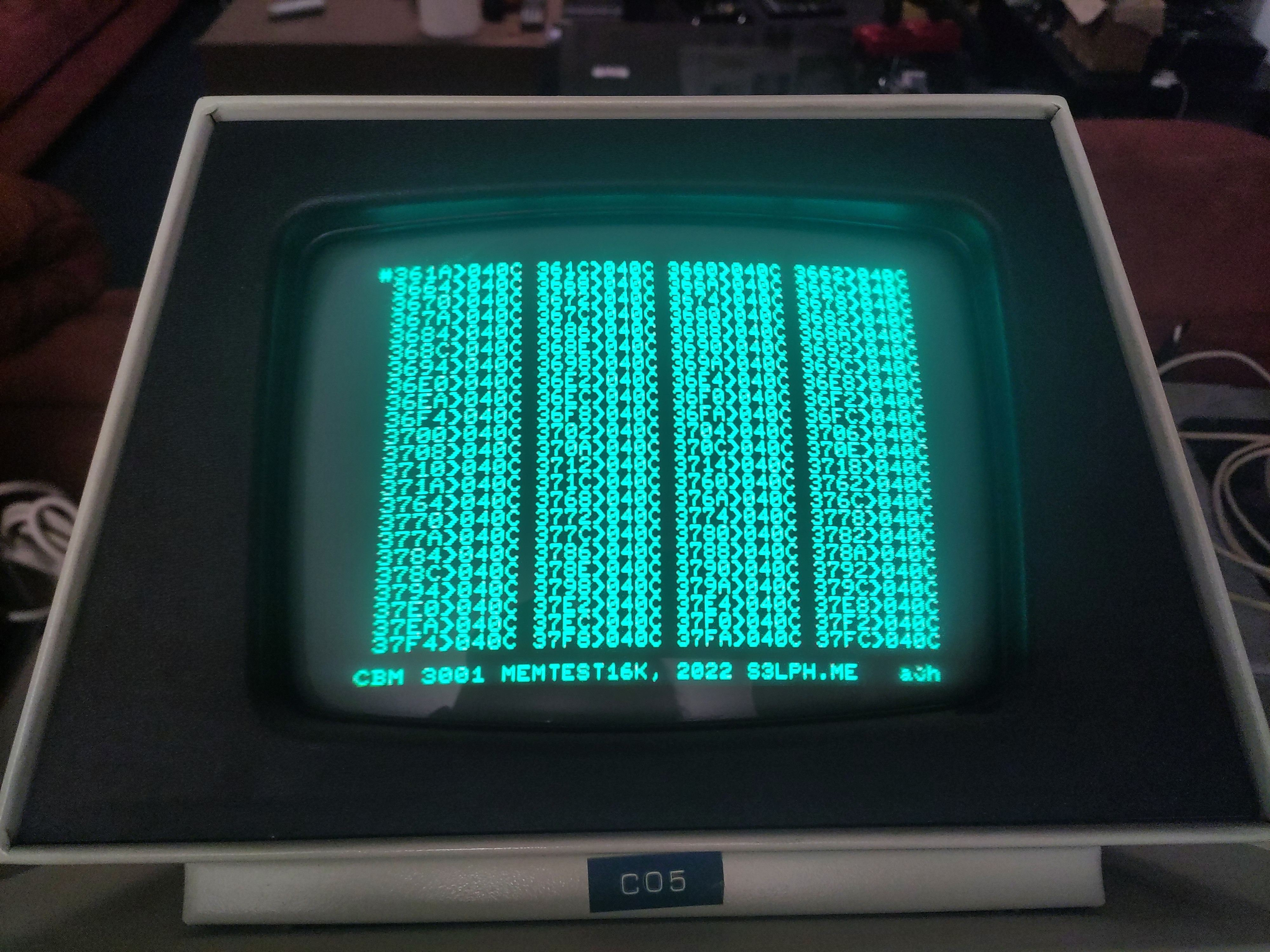
Flashing the memtest16k image to a PROM and booting it on our CBM 3016 revealed memory errors for every single address in the upper half of the DRAM address space, $2000:$3fff. Most of these were indeed caused by the faulty memory module we had already identified earlier, however, there have also been some additional reports caused by a different module, as they had happened at a different bit.
Replacing Defective RAM Modules
We assumed it would be quite hard to find compatible memory modules. However, in our hackerspace I found a Commodore C64 which had already been scavenged for spare parts, so there were no hard feelings in taking its memory as well. The C64 has 8 memory modules, each holding 64Kib. These modules, Micron MT4264-15 were mostly pin-compatible to the MK4108/4116; they have an additional address pin, but fewer power pins (they run on 5V only, rather than the MK4108's triplet of -5V, +5V and +12V). Making an adapter socket was trivial, the hardest part was desoldering the DIP24 package from the C64 PCB; instead of using DIP sockets like in the PET/CBM series, the C64 has its RAM soldered directly to the PCB.
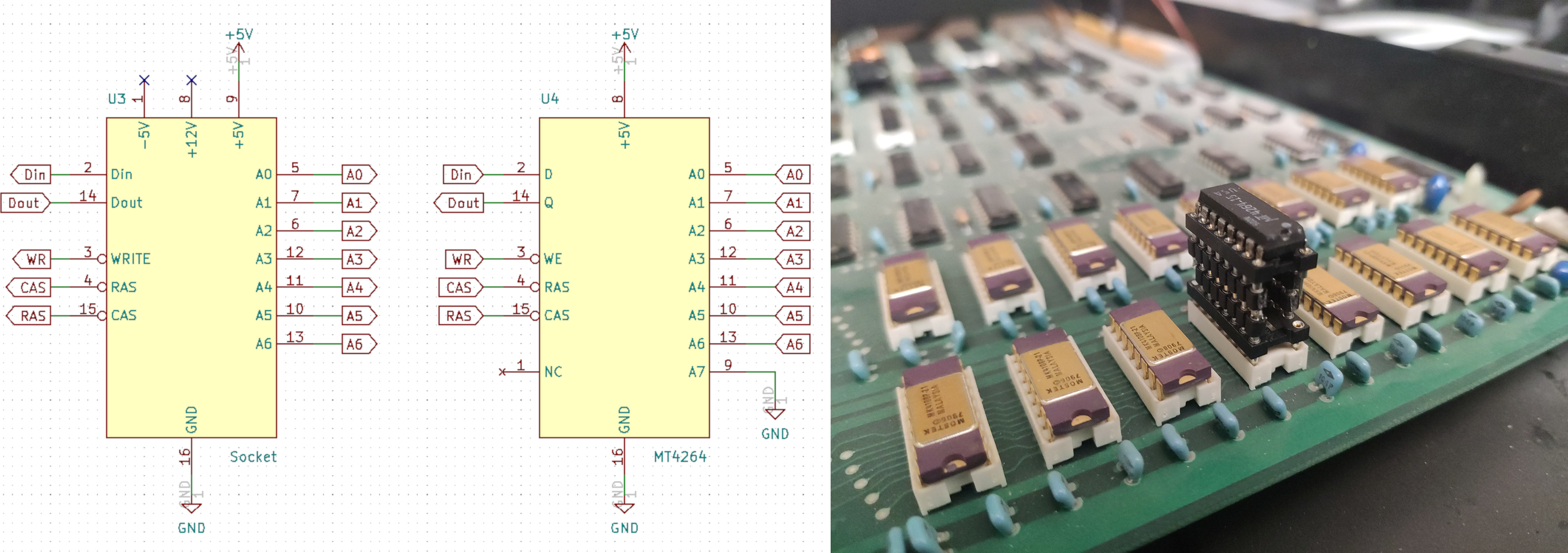
Once we had replaced the one RAM module that was entirely broken, we started another memtest run, and no errors were reported at all. This came as a surprise, since based on the results from previous memtests we assumed two modules had to be faulty. We then reinserted the KERNAL ROM, and finally the CBM 3016 started up with its full memory size available:
